


Pine fun - Device access from the user level
Genode's peripheral device drivers live outside the kernel and have the form of regular user-level components. This article presents how the device-hardware access works under these conditions, while taking the general-purpose I/O pins of the Pine-A64-LTS single-board computer as playground.
In the previous article, we reached a solid base-line of functionality for the kernel and Genode framework on the Pine-A64-LTS board. Now it is time to turn out attention to the main topic of our SoC porting effort, which is the interaction with peripheral devices.
As a warm-up, there is no better peripheral than a general-purpose-I/O pin (GPIO) controller. It is a relatively simple device while enabling us to observe very satisfying physical effects. Despite the simplicity, we are faced with the two most important device-driver-related topics, namely accessing device registers and dispatching interrupts.
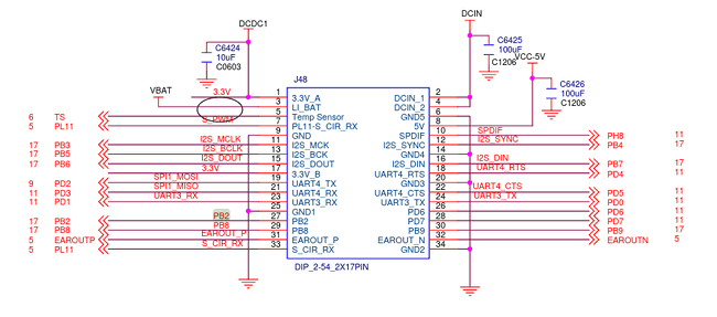
The investigation starts with the quest of finding a suitable pin at one of the various connectors present on the board. The board schematics as found in the PINE64 Wiki are our guide. While skimming the 19 pages of the document and glancing at the headlines above the very technical looking drawings, the so-called Euler connector at page 12 catches my attention because this name appears besides a prominently visible 34-pin header on the board.
|
By looking at the schematics, it is easy to guess that the box with the 34 connectors corresponds to this pin header. The pins have labels, which give us clues about their designated purposes. E.g., some pins are wired to fixed voltages like 5V or 3.3V or ground. Some others hint at specific functionality present in the SoC or another component on the board, e.g., those prefixed with I2S or UART or EAROUT. Some pins however, stand out by being named PB2, PB8, PD7 and such. The prefix P presumably stands for pin. Other usual signal-labeling schemes as found in schematics documents contain the pattern "IO" or "GPIO". Let's settle on the pin PB2 and see where this leads us. By searching the document for "PB2", we can see that the same signal appears at a box labeled "R18" (on the page for the Pi-2 connector). By searching for the ominous component "R18", we quickly learn that this label refers to the Allwinner SoC. So the pin is directly connected to the SoC. Did we ask for more? To sum up our findings, the following pins of the Euler connector are of interest to us:
-
Pin 8: 5V
-
Pin 27: PB2 (wired to the SoC)
-
Pin 34: ground
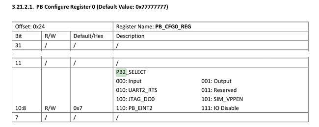
The label PB2 has to have a meaning for the SoC, which is hopefully cleared up in the SoC's documentation. For SoCs with no public documentation, the most compelling alternative source for such information are device-tree source (dts) files as usually provided by the SoC vendors for the Linux kernel and U-Boot. But let us save the device-tree topic for later. Being lucky that the Allwinner A64 SoC documentation is public, we can search it for "PB2", which brings us to Page 377, specifically to the description of a bit field named "PB2_SELECT" at a so-called "PB Configure Register 0".
|
The surrounding Section 3.21 "Port Controller(CPUx-PORT)" gives us the insights we need. PB2 is apparently one of the 10 input/output pins of Port B of the PIO peripheral, which presumably stands for Pin I/O. There exist plenty of device registers that are mirrored for different ports (B, C, D, ...).
Using a GPIO pin for sensing a digital signal
As a first exercise, let's write a little program at allwinner/src/test/pin_state/main.cc that accesses the PB Configure Register 0.
 #include <base/component.h>
 #include <base/log.h>
 #include <base/attached_io_mem_dataspace.h>
 #include <util/mmio.h>

 namespace Test {
     using namespace Genode;
     struct Main;
 }


 struct Test::Main
 {
     Env &_env;

     Attached_io_mem_dataspace _pio_ds { _env, 0x1c20800u, 0x400u };

     struct Pio : Mmio
     {
         struct Pb_cfg0 : Register<0x24, 32>
         {
             struct Pb2_select : Bitfield<8, 3> { };
         };

         Pio(addr_t base) : Mmio(base)
         {
             log("PB2_SELECT: ", read<Pb_cfg0::Pb2_select>());
         }
     };

     Pio _pio { (addr_t)_pio_ds.local_addr<void>() };

     Main(Env &env) : _env(env) { }
 };


 void Component::construct(Genode::Env &env)
 {
     static Test::Main main(env);
 }
The following details are worth noting.
-
The program comes in the form of a Main object as opposed to a main() function. To learn more about this structure, please refer to the article Genode's Conscious C++ dialect.
-
The Env interface allows the code to interact with the environment of the Genode component such as allocating memory, or opening a connection to a service provided by another component.
-
The _pio_ds member opens a connection to an IO_MEM service and obtains a virtual-memory mapping of the specified range of the system bus. The numbers are taken from the Allwinner A64 manual.
-
The Pio struct represents a memory-mapped I/O region, inheriting the Mmio type. The Mmio constructor takes the base address of the underlying device-register range as argument. The structs defined in the scope of the Pio struct mirrors the register structure of the memory-mapped I/O range: There exists a 32-bit wide register Pb_cfg0 at offset 0x24.
struct Pb_cfg0 : Register<0x24, 32>
The bits 8 to 10 of this register correspond to the bit field Pb2_select.
struct Pb2_select : Bitfield<8, 3> { };These declarations correspond one-to-one with the register definitions as found in the SoC user manual.
-
In tho Pio constructor, we print the value of the Pb2_select bitfield by using the Mmio::read method.
log("PB2_SELECT: ", read<Pb_cfg0::Pb2_select>());Note that the code is completely free of (often bug-prone) bit-masking/shifting operations.
To build the program, we have to accompany it with a target.mk file as follows.
 TARGET := test-pin_state
 SRC_CC := main.cc
 LIBS   += base
Finally, we need to embed the program into a Genode system scenario. The following run script accomplishes this.
 build { core init test/pin_state }

 create_boot_directory

 install_config {
   <config>
     <parent-provides>
       <service name="LOG"/>
       <service name="PD"/>
       <service name="CPU"/>
       <service name="ROM"/>
       <service name="IO_MEM"/>
       <service name="IRQ"/>
     </parent-provides>

     <default caps="100"/>

     <start name="test-pin_state">
       <resource name="RAM" quantum="1M"/>
       <route> <any-service> <parent/> </any-service> </route>
     </start>
   </config>
 }

 build_boot_image { core ld.lib.so init test-pin_state }

 run_genode_until forever
When executing this run script, we can observe the following output:
 kernel initialized
 ROM modules:
  ROM: [000000004012c000,000000004012c17f) config
  ROM: [0000000040006000,0000000040007000) core_log
  ROM: [00000000401eb000,000000004022c260) init
  ROM: [000000004012d000,00000000401e4bd0) ld.lib.so
  ROM: [0000000040004000,0000000040005000) platform_info
  ROM: [00000000401e5000,00000000401ea0d0) test-pin_state

 Genode 21.02-61-g446df00d0d8
 2010 MiB RAM and 64533 caps assigned to init
 [init -> test-pin_state] PB2_SELECT: 7
The PB2_SELECT bits have the value 7, which is the default value (I/O disable) according to the documentation. You may ask, what's behind those bits? The number of connectors of a chip is physically limited by the space of the chip's package and the practicalities of PCB routing. To make one SoC applicable to a wide variety of products, SoC vendors implement a feature set much larger than the pin count would allow and leave the selection of a board-specific subset of those features to the board vendor. So different boards can use the same SoC but with different functionality exposed. The ultimate meaning of the physical pins is left to a software configuration. This multiplexing of pins to multiple SoC functionalities is often referred to as I/O muxing or pin muxing. On some SoCs, the I/O mux configuration is presented as a distinct device. On the Allwinner A64, it is part of the PIO device. For the pin PB2, the SoC provides the following options.
 000: Input
 010: UART2_RTS
 100: JTAG_DO0
 110: PB_EINT2
 001: Output
 011: Reserved
 101: SIM_VPPEN
 111: IO Disable    <- default
To sample the state of pin 27 of the Euler connector, we have to change the configuration value to 0 (input). Let's set the configuration value and validate that the change has the desired effect by changing the body of the Pio struct as follows.
 struct Pb_cfg0 : Register<0x24, 32>
 {
     struct Pb2_select : Bitfield<8, 3>
     {
         enum { IN = 0 };
     };
 };

 Pio(addr_t base) : Mmio(base)
 {
     log("PB2_SELECT: ", read<Pb_cfg0::Pb2_select>());

     write<Pb_cfg0::Pb2_select>(Pb_cfg0::Pb2_select::IN);

     log("PB2_SELECT: ", read<Pb_cfg0::Pb2_select>());
 }
Note the enum value definition for IN, which helps us to self-document the code as opposed to just writing the value 0. The output looks as expected. We read back the value that we have just written.
 [init -> test-pin_state] PB2_SELECT: 7
 [init -> test-pin_state] PB2_SELECT: 0
With the PB2 pin configured as input, let's see if we can observe a signal change at the Euler connector pin 27. The pin state is captured by the so-called PB Data Register (PB_DATA_REG) at offset 0x34. The register hosts one bit for each pin of the port B. For the PB2 pin, we have to poll bit 2. Or, to put it in other words:
 ...
 struct Pb_data : Register<0x34, 32>
 {
     struct Pb2 : Bitfield<2, 1> { };
 };

 Pio(addr_t base) : Mmio(base)
 {
     write<Pb_cfg0::Pb2_select>(Pb_cfg0::Pb2_select::IN);

     while (true)
         log("PB2_STATE: ", read<Pb_data::Pb2>());
 }
This gives us the following output:
 [init -> test-pin_state] PB2_STATE: 1
 [init -> test-pin_state] PB2_STATE: 1
 [init -> test-pin_state] PB2_STATE: 0
 [init -> test-pin_state] PB2_STATE: 0
 [init -> test-pin_state] PB2_STATE: 0
 [init -> test-pin_state] PB2_STATE: 1
 [init -> test-pin_state] PB2_STATE: 1
 [init -> test-pin_state] PB2_STATE: 0
 [init -> test-pin_state] PB2_STATE: 0
 [init -> test-pin_state] PB2_STATE: 0
 [init -> test-pin_state] PB2_STATE: 1
 [init -> test-pin_state] PB2_STATE: 1
The pattern looks interesting, like if the PB2 pin is not quite sure about its state. For the experiment, let's try to connect the PB2 pin to ground. That is shorting the pins 27 (PB2) with 34 (GND). As a matter of courtesy, it is good to avoid connecting the pins directly but instead placing a resistor of a few hundred Ohm between both pins. Should we have done a mistake along our way and accidentally connect a 5V pin to GND, the current will flow nicely through our resistor instead of producing a short circuit. So what happens when connecting both pins?
 [init -> test-pin_state] PB2_STATE: 0
 [init -> test-pin_state] PB2_STATE: 0
 [init -> test-pin_state] PB2_STATE: 0
 [init -> test-pin_state] PB2_STATE: 0
 [init -> test-pin_state] PB2_STATE: 0
 [init -> test-pin_state] PB2_STATE: 0
 [init -> test-pin_state] PB2_STATE: 0
 ...
That looks clean! What about connecting pin 27 (PB2) to pin 8 (5V)?
 [init -> test-pin_state] PB2_STATE: 1
 [init -> test-pin_state] PB2_STATE: 1
 [init -> test-pin_state] PB2_STATE: 1
 [init -> test-pin_state] PB2_STATE: 1
 [init -> test-pin_state] PB2_STATE: 1
 [init -> test-pin_state] PB2_STATE: 1
 ...
Isn't that wonderful?
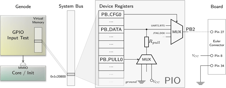
The following picture summarizes our scenario.
|
The pin 27 of the Euler connector goes to the PB2 pin of the SoC. Via the PB_CFG0 register, we configure this pin to be used as general-purpose I/O pin reflected by bit 2 in the PB_DATA register. The register set of the PIO device unit is visible at physical address 0x1c20800 at the system bus. Thanks to the MMIO service of Genode's core, our test component becomes able to access this register range as part of its virtual address space. So what's this PB_PULL0 register shown in the picture?
This register can be used to prevent the fluctuating state when leaving the PB2 pin unconnected. Jargon speaks of high impedance, which sounds super educated but means the same thing. In real-world applications, this floating state is often not wanted. After all, digital means 0 or 1 but not maybe. Fortunately, the state can easily be avoided by connecting the PB2 pin via a very high resistor to ground (or 5V). This resistor pulls the floating potential down to ground (or up to 5V). Since this is such a common need, the SoC comes readily equipped with pull-down or pull-up resistors. We just need to enable either option, which can be done via the PB PULL Register 0 (PB_PULL0).
 ...
 struct Pb_pull0 : Register<0x40, 32>
 {
     enum { PULL_DOWN = 2 };

     struct Pb2 : Bitfield<4, 2> { };
 };

 Pio(addr_t base) : Mmio(base)
 {
     ...
     write<Pb_pull0::Pb2>(Pb_pull0::PULL_DOWN);
     ...
 }
With this little change, the output stays at 0 even when leaving the pin 27 (PB2) disconnected.
Driving an LED via a GPIO pin
Let's try the reverse, using the PB2 pin as a digital output signal. At this point, it is easy to connect the dots at the software side.
-
Configure the PB2_SELECT bits of the PB_CFG0 register to operate the pin in output mode, which is value 1.
-
Write the desired state to the bit 2 of the PB_DATA register.
The following code sets up the PB_CFG0 register and equips the Pio struct with a toggle_pb2 method that reads the PB2 state from the PB_DATA register and writes back the inverted state.
 struct Pio : Mmio
 {
     struct Pb_cfg0 : Register<0x24, 32>
     {
         struct Pb2_select : Bitfield<8, 3>
         {
             enum { OUT = 1 };
         };
     };

     struct Pb_data : Register<0x34, 32>
     {
         struct Pb2 : Bitfield<2, 1> { };
     };

     Pio(addr_t base) : Mmio(base)
     {
         /* configure PB2 pin to output mode */
         write<Pb_cfg0::Pb2_select>(Pb_cfg0::Pb2_select::OUT);
     }

     void toggle_pb2()
     {
         bool const value = read<Pb_data::Pb2>();

         /* write back inverted value */
         write<Pb_data::Pb2>(!value);
     }
 };
To let the test program blink the LED at a visible rate, we need a timer mechanism. Here, Genode's Timer::Connection becomes handy. By adding following few lines to the Main object, the toggle_pb2 method gets called every 250 milliseconds.
 #include <timer_session/connection.h>
 ...
 struct Main
 {
     Timer::Connection _timer { _env };

     void _handle_timeout(Duration)
     {
         _pio.toggle_pb2();
     }

     Timer::Periodic_timeout<Main> _timout_handler {
         _timer, *this, &Main::_handle_timeout, Microseconds { 250*1000 } };
 };
Until now, the simple test scenario lack a timer service. So we have to extend the run script a bit.
-
Adding the timer service to the list of components to build.
build { ... timer } -
Adding a start node to the static system configuration.
 <start name="timer">
   <resource name="RAM" quantum="1M"/>
   <route> <any-service> <parent/> </any-service> </route>
   <provides> <service name="Timer"/> </provides>
 </start>
-
Routing the timer-session request by the test program to the timer service.
<start name="test-pin_control"> <resource name="RAM" quantum="1M"/> <route> <service name="Timer"> <child name="timer"/> </service> <any-service> <parent/> </any-service> </route> </start> -
Adding the timer executable to the boot image.
build_boot_image { ... timer }
At the hardware side, we need to connect an LED in series with a resistor dimensioned such that the potential difference over the LED will be approximately 2V. When connecting a 5V pin over the LED and the resistor to ground, the resistor should hence take away 3V. Most LEDs draw a current of 20mA. Hence, Ohm's law (R = U / I) tells us that the resistor should have a value of 3V / 0.02 A = 15O Ohm. Picking a higher resistor cannot hurt. It will just reduce the brightness of the LED. Long story short, a resistor of a few hundred Ohm should be fine.
If any electrical engineer is reading this and finds I'm writing nonsense, please contact me.
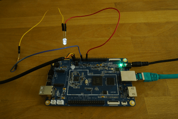
To see if the LED is able to light up in principle when connected with the resistor in series, the pins 8 (5V) and 34 (GND) become handy. The anode contact (the long one) of the LED must face the 5V side.
Now its time to bring software and hardware together by connecting the LED's anode to pin 27 (PB2) and starting the test program. The final setup looks like this. What's not captured in the photo is that the LED is indeed blinking.
|
Responding to device interrupts
Besides sensing and driving digital signals, GPIO pins are often used as an interrupt source. So some external circuity can trigger a sporadic response by the software.
To explore the interrupt facility, let's first ignore the ARM GIC interrupt controller for a moment and just focus on the PIO device. In the PB_CFG0 register, the value 6 configures the pin as operating in PB_EINT2 mode. Whatever the meaning of the E or the 2, the pattern "INT" hints at what we want.
 ...
 struct Pb_cfg0 : Register<0x24, 32>
 {
     struct Pb2_select : Bitfield<8, 3>
     {
         enum { EINT2 = 6 };
     };
 };
 ...
 Pio(addr_t base) : Mmio(base)
 {
     write<Pb_pull0::Pb2>(Pb_pull0::PULL_DOWN);

     write<Pb_cfg0::Pb2_select>(Pb_cfg0::Pb2_select::EINT2);
 }
The PB External Interrupt Status Register (PB_EINT_STATUS_REG) reflects the interrupt state.
struct Pb_eint_status : Register<0x214, 32> { };
As an intermediate test, we can poll this register and see what happens when we connect the pin 27 (PB2) to pin 8 (5V). The polling loop can be directly added to the Pio constructor.
 while (true)
     log("PB_EINT_STATUS: ", read<Pb_eint_status>());
After starting the program, we see the following output scrolling by.
 [init -> test-pin_interrupt] PB_EINT_STATUS: 0
 [init -> test-pin_interrupt] PB_EINT_STATUS: 0
 [init -> test-pin_interrupt] PB_EINT_STATUS: 0
 ...
Once after connecting PB2 to 5V, the output changes to:
 [init -> test-pin_interrupt] PB_EINT_STATUS: 4
 [init -> test-pin_interrupt] PB_EINT_STATUS: 4
 [init -> test-pin_interrupt] PB_EINT_STATUS: 4
 ...
The 4 corresponds to the bit 2 set, which is what we anticipated. The status bit never returns to the original state. To clear the bit, a 1 must be written to the status bit. This can be tested by slightly changing the while loop.
 while (true) {
     if (read<Pb_eint_status::Pb2>()) {
         log("PB2 EINT status went high");
         write<Pb_eint_status::Pb2>(1);
     }
 }
The scrolling log output is no more. Now, we see only one message each time we fiddle with the PB2 pin.
[init -> test-pin_interrupt] PB2 EINT status went high
The clearing of the interrupt status works as advertised.
Until now, we have observed the PIO device behavior via a polling loop, which is of course not in the spirit of using interrupts. To complete the scenario, we have to tell the PIO to inform the CPU's interrupt controller (GIC) whenever the EINT status goes high. The connection between the PIO and the GIC can be established via the PB External Interrupt Control Register.
 struct Pb_eint_ctl : Register<0x210, 32>
 {
    struct Pb2 : Bitfield<2, 1> { };
 };
When setting bit 2 in this register, the GIC will see a device interrupt from the PIO device. The GIC interrupt numbers are documented in the Allwinner A64 manual at page 211. PB_EINT is interrupt number 43.
To obtain an interrupt in our component, we can use core's IRQ service as follows.
 #include <irq_session/connection.h>
 ...

 struct Test::Main
 {
     ...

     enum { PB_EINT = 43 };

     Irq_connection _irq { _env, PB_EINT };


     unsigned _count = 0;

     void _handle_irq()
     {
         log("interrupt ", _count++, " occurred");

         _pio.clear_pb2_status();

         _irq.ack_irq();
     }

     Signal_handler<Main> _irq_handler { _env.ep(), *this, &Main::_handle_irq };

     Main(Env &env) : _env(env)
     {
         _irq.sigh(_irq_handler);
         _handle_irq();
     }
 };
The following details about this code fragment are worth highlighting.
-
The GIC interrupt number is passed as argument to the IRQ connection to core.
-
Interrupts are delivered as signals. The _irq_handler is a signal handler that is registered at the IRQ session via the _irq.sigh method. Each time the signal occurs, the Main::_handle_irq method is executed.
-
The _pio.clear_pb2_status method performs the clearing of the PB2 interrupt status.
 struct Pio
 {
      ...
      void clear_pb2_status()
      {
          write<Pb_eint_status::Pb2>(1);
      }
 };
The _irq.ack_irq call acknowledges the interrupt at the GIC.
-
The _handle_irq method is manually called once after registering the signal handler at the IRQ session. This pattern ensures that an initially pending interrupt that occurred just before the call of _irq.sigh is processed before the component goes into idle state.
The following illustration summarizes the scenario.
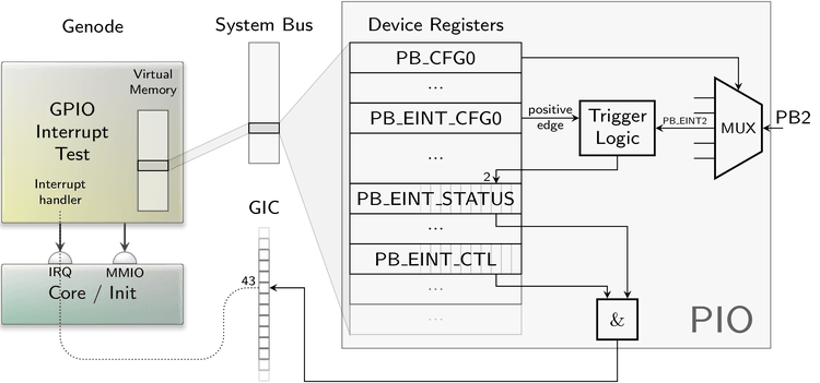
|
The exact conditions for triggering an interrupt can be configured for the pin using the PB External Interrupt Configure Register 0 (PB_EINT_CFG0). By default, the status goes to 1 as soon as a rising edge is detected. The other alternatives are falling edge, level-high (interrupt stays pending as long as the signal is high), level-low, and double edge (interrupt on any change of the signal).
Only if the bit 2 of the status register (PB_EINT_STATUS) and the bit 2 of the control register (PB_EINT_CTL) are set, the interrupt controller (GIC) receives an interrupt. This GIC interrupt (number 43) is propagated via core's IRQ service to our user-level component, which implements the interrupt handler.
Thanks to the interrupt mechanism, we can now respond to sporadic hardware events without active polling. When executing the scenario, we can see that a single message occurs each time when fiddling with the PB2 pin. The system stays completely idle otherwise.
 [init -> test-pin_interrupt] interrupt 0 occurred
 [init -> test-pin_interrupt] interrupt 1 occurred
 [init -> test-pin_interrupt] interrupt 2 occurred
 [init -> test-pin_interrupt] interrupt 3 occurred
 [init -> test-pin_interrupt] interrupt 4 occurred
Public repository
The test programs described above can be found at the genode-allwinner Git repository. The C++ code is located at src/test/pin_state/, src/test/pin_control/, and src/test/pin_interrupt/. These test programs are accompanied with matching run scripts located at the run/ directory.
In the next part, we mold the results of the experiments into a proper driver component. Read on...